Marktech Optoelectronics has announced a significant expansion of its silicon photodiode portfolio, introducing larger active-area detectors designed to enhance sensitivity, signal strength, and alignment precision across a wide range of advanced optical applications. The move strengthens the company’s position in photodetector technologies used in fields spanning space systems, analytical instrumentation, biomedical diagnostics, and nanoscale research.
The expanded lineup includes both single-element silicon photodiodes and a broadened family of silicon quadrant photodiodes (Si QPDs), featuring substantially larger active areas than Marktech’s previous offerings. According to the company, the increase in optical capture area enables superior low-light detection and improved positional accuracy, particularly in systems where beam divergence, weak signals, or alignment tolerance present technical challenges.
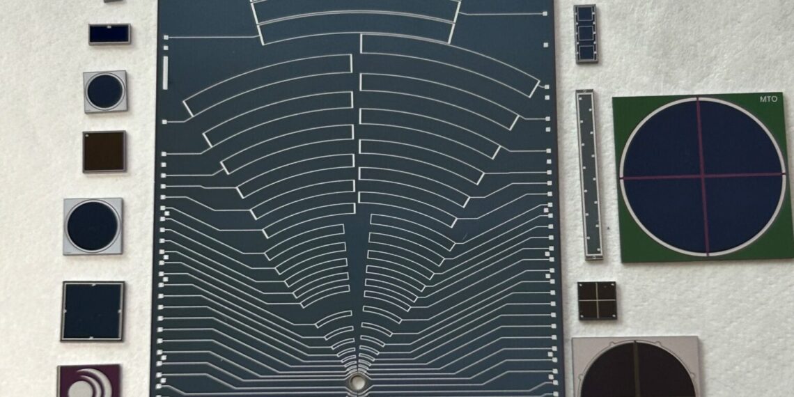
In addition to discrete detectors, Marktech has demonstrated the capability to manufacture extremely large active-area silicon photodiode arrays, including complex multi-element configurations such as a 64-element array. Many of these arrays incorporate the company’s proprietary cross-talk-reduction technology, aimed at improving signal integrity between adjacent elements—an important factor in high-resolution sensing and imaging systems.
Manufacturing and process control remain central to the company’s strategy. Marktech’s silicon photodiodes are produced entirely in the United States, with silicon device fabrication, packaging, and final testing carried out at its Marktech West facility in Simi Valley, California. Engineering and marketing operations are based in Latham, New York. This vertically integrated approach, the company says, enables consistent quality, high reliability, and repeatable performance for demanding applications.
“Larger active areas fundamentally change what’s possible in optical detection,” said Barry Jones, Marktech West Business Manager and silicon photodiode specialist. By capturing more incident photons, Jones explained, the detectors generate higher signal levels and can detect lower light inputs than smaller devices, an advantage in applications such as spectrophotometry, fluorimetry, biomedical diagnostics, and environmental monitoring. In quadrant configurations, larger areas also provide improved tolerance to misalignment and better detection of large or weak optical beams.
The newly expanded silicon photodiodes deliver responsivity across a broad 250–1100 nm spectral range, with peak performance optimized in the near-infrared, ultraviolet A, blue-green, and visible regions. This spectral coverage supports applications including NIR beam alignment, colorimetry, optical feedback systems, and precision metrology.
A key focus of the announcement is the expanded silicon quadrant photodiode family. Marktech now offers devices with active areas of 5.8 mm², 25 mm², and 50 mm², with a 100 mm² quadrant photodiode currently under development. Compared with the baseline device, these represent approximately 4.3× to 17.2× increases in optical capture area, enabling greater precision in beam positioning, tracking, nulling, and alignment tasks.
Quadrant photodiodes play a critical role across vastly different scales. In space systems, fine sun sensors use quadrant detectors to determine a satellite’s orientation relative to the sun, supporting attitude control and navigation in orbit. At the opposite extreme, atomic force microscopes rely on quadrant photodiodes to measure nanometer-scale cantilever deflections, allowing researchers to image surfaces at atomic resolution.
Complementing the quadrant portfolio, Marktech has introduced new large active-area single-element silicon photodiodes engineered for high sensitivity, stability, and low noise. These detectors are housed in hermetic TO-can packages designed to maintain performance under harsh environmental conditions. The company also offers custom packaging options, including ceramic SAW packages, its proprietary hermetic ATLAS surface-mount design, and hybrid configurations that co-package photodiodes with transimpedance amplifiers or thermoelectric coolers.
The large active-area single-element detectors are optimized for enhanced sensitivity in the 300–560 nm range, including 365 nm UVA and blue-green wavelengths. Target applications include fire and flame sensing, fluorescence measurement, spectrometry, document authentication, and gas detection for species such as nitrogen dioxide and ozone. As with most large-area photodiodes, Marktech notes that increased area can reduce bandwidth compared to smaller devices, a trade-off system designers must consider depending on speed requirements.
Beyond silicon’s intrinsic 1100 nm wavelength limit, Marktech continues to offer extended spectral solutions. These include indium gallium arsenide (InGaAs) photodiodes with cutoff wavelengths of 1.7 µm and 2.6 µm, as well as dual-chip silicon–InGaAs detectors that provide ultra-broadband coverage from 250 to 2600 nm. The InGaAs components for these dual-chip detectors are produced by Optrans Corporation in Kawasaki-Shi, Japan, which maintains in-house capabilities from epitaxial wafer growth through advanced packaging.
The company also supplies silicon carbide photodiodes for deep ultraviolet detection below 250 nm, as well as a broad range of custom detector solutions. These include multi-element arrays, tailored peak responsivity, integrated optical filters, precision-aligned multi-chip assemblies, and hybridized detectors incorporating cooling and amplification electronics.
According to Marktech, the expanded detector platform is intended to support innovation across industries including optical communications, robotics, medical imaging, environmental monitoring, spectroscopy, drone navigation, and precision motion control.