Renesas Electronics Corporation (TSE:6723) has developed three new System-on-Chip (SoC) technologies for automotive multi-domain electronic control units (ECUs), aimed at supporting the transition to software-defined vehicles (SDVs). The company presented the technologies at the International Solid-State Circuits Conference 2026, held February 15–19 in San Francisco.
As vehicle architectures shift toward centralized computing, automotive SoCs are required to run multiple applications simultaneously while meeting stringent functional safety standards. Increasing integration and AI processing demands are also driving greater power consumption and design complexity. Renesas stated that its latest developments focus on scalability, AI performance, power efficiency, and safety compliance for next-generation electrical/electronic (E/E) architectures.
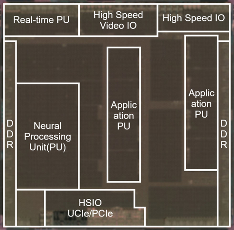
One of the key advances is a proprietary chiplet architecture designed to support ASIL D functional safety requirements. The architecture combines the standard UCIe die-to-die interface with a proprietary RegionID mechanism to achieve Freedom from Interference (FFI) when multiple applications operate concurrently. Because conventional UCIe interfaces do not transmit RegionIDs across dies, Renesas developed a method to map RegionIDs into physical address space, encode them into the UCIe region, and transmit them between chiplets. This enables secure access control via the memory management unit and real-time cores while maintaining compliance with automotive safety standards. The company reported transmission speeds of 51.2 GB/s, approaching the upper limits of intra-SoC bandwidth.
Renesas also introduced a 3 nm SoC design to enhance neural processing unit (NPU) performance for AI workloads. As NPUs have expanded in size—approximately 1.5 times larger than previous generations—clock latency has become a growing challenge. To address this, the company redesigned its clock architecture by deploying mini clock pulse generators at the sub-module level rather than at the module level. This reduces clock latency and supports timing requirements for high-performance AI processing.
To maintain automotive-grade quality, Renesas integrated test circuits into the hierarchical clock structure and unified user and test clock signal paths. In test mode, upper- and lower-level clock generators synchronize under a single clock source, enabling phase alignment and supporting zero-defect quality objectives.
In addition, Renesas developed advanced power control technologies incorporating more than 90 power domains. The system enables precise power management ranging from milliwatts to tens of watts depending on operating conditions. Power switches were divided into ring and row configurations to reduce IR drops associated with increased current density in smaller process nodes. According to Renesas, this design reduces IR drops by approximately 13% compared to conventional approaches. A dual core lock step configuration with independent power controls enhances ASIL D compliance, while loopback monitoring and a temperature-resistant digital voltage monitor improve fault detection and aging tolerance.
The new technologies are being deployed in Renesas’ R-Car X5H SoC for automotive multi-domain ECUs, supporting applications such as autonomous driving and digital cockpit systems.