Bruker Corporation has announced accelerated development of its photothermal AFM-IR spectroscopy capabilities, aiming to address emerging research challenges in the semiconductor industry as device architectures become smaller and more complex.
The company, a leading supplier of nanoscale infrared (nanoIR) spectroscopy technology, is expanding the application of AFM-IR beyond contamination analysis into advanced research areas. These include extreme ultraviolet (EUV) photoresist patterning, next-generation transistor materials, and site-selective surface functionalization at the nanoscale. These domains are critical for enabling future semiconductor innovations and improving device performance.
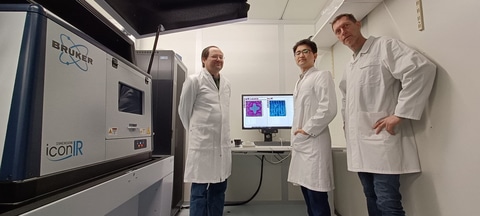
As part of this effort, Bruker has entered into a Joint Development Project with imec, a global research and innovation hub for advanced semiconductor technologies. Under the collaboration, Bruker has installed its Dimension IconIR system at imec to evaluate the effectiveness of photothermal AFM-IR in addressing complex nanoscale research challenges.
The project focuses on leveraging nanoscale chemical characterization to better understand material behavior and interfaces, which are key factors in semiconductor process development. Researchers aim to assess how this technology can provide deeper insights into material interactions that influence device scaling and performance.
Albert Minj, senior researcher at imec, said the collaboration reflects evolving metrology needs in semiconductor research. He noted that the IconIR system enables label-free chemical analysis with sub-5 nanometer resolution, supporting detailed study of EUV resist chemistry and advanced materials.
David V. Rossi, President of Bruker’s Nano Surfaces and Metrology Division, said the partnership will expand the role of photothermal AFM-IR in semiconductor environments. He added that nanoscale infrared spectroscopy can deliver chemical insights not accessible through conventional techniques.