In a breakthrough that addresses a decades-old question in semiconductor physics, a joint research team led by Mitsubishi Electric Corporation has, for the first time, clarified the mechanism by which hydrogen generates free electrons in silicon through interactions with crystal defects. The findings, published on January 13 in Communications Materials, a journal from the Nature Portfolio, are expected to influence the future design of power semiconductors and may extend to emerging ultra-wide bandgap (UWBG) materials such as diamond.
The research was conducted collaboratively by Mitsubishi Electric, the Institute of Science Tokyo, the University of Tsukuba, and Quemix Corporation. It provides long-sought clarity on a phenomenon that has been exploited in semiconductor manufacturing for nearly half a century without a complete theoretical explanation.
Hydrogen ion implantation has long been used to control electron concentration in silicon, particularly for forming n-type layers in power devices such as insulated gate bipolar transistors (IGBTs). These components play a central role in power conversion systems used in electric vehicles, renewable energy infrastructure, and industrial equipment. Improving their efficiency is considered critical as countries push toward carbon neutrality. Despite its widespread use, however, the fundamental reason hydrogen could increase free-electron concentration in silicon had remained unresolved.
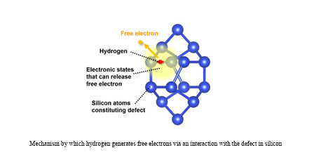
Earlier work in 2023 by Mitsubishi Electric and the University of Tsukuba identified a specific defect in silicon, known as the I4 defect, as being closely linked to electron generation. This defect is formed when extra silicon atoms disrupt the regular crystal lattice. While researchers confirmed that hydrogen binds to this defect complex, the precise mechanism by which free electrons were released was still unclear.
The latest study bridges that gap. Using advanced first-principles calculations based on density functional theory, researchers from the Institute of Science Tokyo and Quemix modeled how hydrogen atoms behave around the I4 defect. Their calculations showed that hydrogen alone, when embedded in defect-free silicon, does not generate free electrons. The situation changes, however, when hydrogen interacts with the I4 defect.
According to the study, hydrogen atoms can occupy bond-center positions between silicon atoms near the defect. In this configuration, the electronic structure of the defect shifts in a way that promotes electron release. Further molecular orbital analysis revealed a cooperative mechanism: an electron associated with hydrogen transfers to the defect, and the defect, in turn, releases an electron into the silicon lattice as a free carrier. This interaction between hydrogen and the defect explains experimental observations that had puzzled researchers for decades.
Beyond the fundamental insight, the work has direct implications for device performance. Mitsubishi Electric reported that combining hydrogen ion implantation with thinner silicon substrates has already led to measurable efficiency gains. In 1,200-volt-class devices, the company has demonstrated total power loss reductions of approximately 10% in IGBTs and 20% in diodes compared with its seventh-generation products. The newly clarified mechanism underpins these improvements by enabling more precise control of electron concentration.
The research may also have broader significance beyond silicon. UWBG materials such as diamond and aluminum nitride are seen as promising candidates for next-generation power electronics and quantum sensors due to their superior breakdown strength and thermal properties. However, controlling electron concentration in these materials has proven extremely challenging. Preliminary calculations suggest that a similar hydrogen-defect interaction could occur in diamond, where hydrogen prefers bond-center positions between carbon atoms. If paired defects are present, a comparable free-electron generation mechanism may be possible.
While the findings remain theoretical for UWBG materials, they offer a potential pathway toward overcoming one of the key barriers to their practical adoption. The researchers note that further experimental validation will be required.
The work was supported by grants from the Japan Society for the Promotion of Science and the Japan Science and Technology Agency. Looking ahead, the research team aims to apply this mechanism to a wider range of semiconductor materials, supporting the development of more efficient power devices, high-frequency electronics, and quantum sensing technologies—areas expected to play a vital role in a carbon-neutral future.