Advanced Chip and Circuit Materials (ACCM) has launched two new materials, Celeritas HM50 and Celeritas HM001, aimed at addressing critical challenges in large-format AI chip packaging. The development comes as the semiconductor industry faces increasing pressure to scale AI accelerators while maintaining reliability and performance.
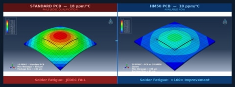
As AI chips grow larger and more complex, thermal mismatch has emerged as a key constraint. Silicon typically has a coefficient of thermal expansion (CTE) of 2–4 ppm/°C. In comparison, standard printed circuit board (PCB) materials operate at around 18 ppm/°C. This difference creates stress during thermal cycling. The result is warpage, package bow, and solder joint fatigue. These issues can reduce manufacturing yield and affect long-term system reliability.
At the same time, rising data rates are placing new demands on signal integrity. Technologies such as high-bandwidth memory (HBM), Universal Chiplet Interconnect Express (UCIe), and chip-to-chip interconnects are now operating at speeds exceeding 100 Gbps. Conventional PCB dielectrics are struggling to keep up. Signal loss and instability are becoming significant barriers to performance.
ACCM’s Celeritas material platform is designed to address both of these challenges. Celeritas HM50 is a negative CTE material, rated at −8 ppm/°C. It is intended for use in power and ground plane layers. When integrated into a PCB stackup, it reduces the overall thermal expansion of the board. This helps bring the board’s behavior closer to that of silicon.
Celeritas HM001 complements this approach. It offers near-zero CTE performance, ranging from −2 to 4 ppm/°C. It is designed for high-speed signal layers. The material features a dielectric constant (Dk) of 2.90 and a loss factor (Df) of 0.001, classified as Tier 9. This enables stable signal transmission at high frequencies and supports data rates above 100 Gbps.
When used together, the two materials allow designers to reduce board-level CTE to below 10 ppm/°C. At the same time, they improve electrical performance across the stackup. This dual capability addresses two major constraints in AI chip design with a single material system.
Keshav Amla, Chief Operating Officer at ACCM, said the company has focused on solving fundamental material limitations rather than making incremental design adjustments. He explained that HM50 is used to control thermomechanical behavior, while HM001 is optimized for signal integrity. This layer-specific approach allows engineers to tailor stackups more precisely to performance requirements.
Performance data provided by the company highlights the potential impact of the materials. HM50 can reduce warpage by 64% and package bow by 81% compared to conventional high-speed materials. It also delivers more than a 100-fold improvement in solder fatigue life. These gains can help designs meet or exceed JEDEC reliability standards, which are becoming harder to achieve as chip complexity increases.
The company also positions its solution as an alternative to glass substrates, which have been proposed as a way to manage thermal expansion. While glass offers some benefits in terms of CTE, it does not address signal integrity challenges to the same extent, according to ACCM.
Both Celeritas HM50 and HM001 are now commercially available. They can be ordered, sampled, and qualified through ACCM’s manufacturing facility in Wisconsin.
The launch reflects a broader shift in the semiconductor industry. As AI workloads continue to expand, the physical limits of materials are becoming more visible. Larger chips, higher data rates, and tighter integration are pushing existing technologies to their limits. In this context, material innovation is emerging as a critical enabler of future performance.