Keysight Technologies (NYSE: KEYS) has launched 3D Interconnect Designer. The tool expands its Electronic Design Automation (EDA) portfolio. It targets advanced chiplet and 3DIC package designs used in AI infrastructure and data centers.
Chiplet architectures are becoming mainstream. Multi-die and stacked-die systems are now common in high-performance computing. These designs require complex 3D interconnect structures. Traditional workflows often struggle to handle this complexity.
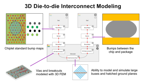
Engineers must manually optimize vias, transmission lines, solder balls and micro-bumps. They must also maintain signal and power integrity in tightly packed layouts. This process is time-consuming. It often leads to multiple design iterations. Development cycles become longer. Costs increase.
Keysight’s new solution introduces a dedicated workflow for 3D interconnect design. It automates critical steps. It reduces manual optimization. The tool handles complex geometries, including hatched and waffled ground planes. These structures are essential in advanced silicon packaging, including interposers and bridge-based designs.
The company says the platform enables faster design, optimization and validation. It is built for chiplets and three-dimensional integrated circuits. The goal is to minimize design spins and improve first-pass success.
Keysight highlights several benefits. The software accelerates design cycles through automation. It reduces human error. It validates compliance early in the lifecycle. The tool supports emerging standards such as UCIe and BoW. It also evaluates Voltage Transfer Function metrics. Early validation lowers the risk of late-stage failures and costly redesigns.
The solution uses electromagnetic-based simulation. This allows detailed electrical analysis of printed circuit boards and package-level interconnects. Engineers can predict performance more accurately. This is critical in high-speed AI and data center systems.
3D Interconnect Designer integrates with Keysight’s broader EDA suite. It also supports standalone deployment. When paired with Chiplet PHY Designer, engineers can further optimize chiplet and 3DIC interconnects.
Nilesh Kamdar, General Manager of EDA Design and Verification at Keysight, said manual optimization has become a bottleneck. He noted that early insight into signal and power integrity challenges helps teams deliver compliant products faster.