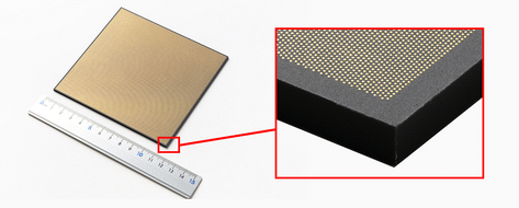
Kyocera Corporation has announced the commercialization of a multilayer ceramic core substrate designed to support next-generation semiconductor packages used in AI data center applications. The company said the product will be formally unveiled at ECTC 2026, scheduled to take place in Orlando, Florida, from May 26 to 29, 2026.
The new substrate is engineered for advanced semiconductor packages, including xPUs—such as CPUs and GPUs—and switch ASICs, which are becoming increasingly complex as AI workloads scale. Built using Kyocera’s proprietary Fine Ceramic materials, the substrate is designed to enable high-density wiring while maintaining structural rigidity, addressing key limitations in conventional packaging technologies.
According to the company, one of the primary advantages of the multilayer ceramic core is its resistance to deformation, commonly referred to as warpage. This issue has become more pronounced as semiconductor packages increase in size and complexity, particularly in high-performance computing environments. By minimizing warpage, the new substrate is expected to improve both performance stability and long-term reliability.
The product also introduces a multilayer ceramic structure that supports finer, three-dimensional wiring. Unlike traditional organic substrates that rely on drilling processes, Kyocera’s approach forms conductive vias while the ceramic material is still pliable. This enables smaller via diameters and tighter spacing, allowing for greater circuit density and improved signal performance in compact designs.
The development comes amid rapid growth in generative AI and large language models, which are driving demand for more powerful processing units and advanced packaging techniques such as 2.5D integration. In these architectures, multiple chips are placed side by side on high-density interposers, increasing the need for substrates that can handle both mechanical stress and dense interconnects.
Kyocera said its ceramic-based solution addresses the performance bottlenecks associated with organic core substrates, particularly in larger formats where deformation and wiring limitations can impact efficiency. The company’s simulations indicate that the new substrate can support thinner designs while maintaining structural integrity, enabling further miniaturization without compromising performance.
In addition to its physical attributes, the substrate supports custom design requirements through simulation capabilities during the development phase. Kyocera provides thermal, electrical, and warpage analysis based on specific device and mounting conditions, helping customers optimize performance before production.