Rambus Inc. (NASDAQ: RMBS) has introduced its PCIe 7.0 Switch IP with Time Division Multiplexing (TDM), expanding its interconnect portfolio to address growing data movement challenges in AI, cloud, and high-performance computing (HPC) systems.
The launch comes as AI infrastructure scales rapidly, increasing pressure on system architectures to handle large volumes of data efficiently. Modern workloads require seamless communication between CPUs, GPUs, accelerators, and NVMe storage. This has made bandwidth optimization, low latency, and efficient interconnect design critical priorities for system developers.
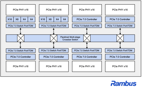
Rambus said its PCIe 7.0 Switch IP is designed to improve link utilization while maintaining deterministic performance. The integration of TDM technology allows traffic to be scheduled and multiplexed across shared links. This enables more efficient use of existing bandwidth without requiring additional physical resources. The approach supports emerging disaggregated and pooled compute architectures, which are becoming central to next-generation data center design.
Built on the PCIe 7.0 specification, the switch IP is optimized for advanced system-on-chip (SoC) platforms used in AI and data center environments. These platforms demand high bandwidth density, advanced traffic management, and scalability to support diverse workloads. The solution is designed to handle both large-scale AI training tasks and latency-sensitive inference operations.
Simon Blake-Wilson, Senior Vice President and General Manager of Silicon IP at Rambus, said AI is reshaping system architecture at a fundamental level. He noted that scaling performance is no longer just about adding more lanes or endpoints. Instead, efficient data orchestration across the system has become essential. He added that the new switch IP provides system designers with greater flexibility to scale bandwidth while reducing complexity and improving overall utilization.
Industry observers highlight that interconnect efficiency is becoming a defining factor in AI infrastructure performance. Jeff Janukowicz, Vice President, Semiconductors and Enabling Technologies, said the ability to move data efficiently between heterogeneous compute and memory resources is now central to building scalable AI platforms. He noted that advanced PCIe switching technologies will play a key role in improving link utilization and enabling flexible traffic management.
The Rambus PCIe 7.0 Switch IP is designed for seamless integration into leading-edge ASIC platforms. It complements the company’s broader PCIe 7.0 portfolio, which includes controllers, retimers, and debug solutions. Together, these offerings aim to help customers accelerate time to market while meeting performance, power, and reliability requirements.
The launch reflects a broader shift in the semiconductor industry toward system-level optimization. As AI and HPC workloads grow more complex, efficient data movement is becoming as important as raw compute power. Interconnect innovation is emerging as a key area of differentiation.
Rambus said the new switch IP reinforces its position in high-speed interface technologies. The company continues to focus on delivering solutions that address the evolving demands of AI, cloud, and HPC infrastructure, where scalability, efficiency, and performance remain critical.