

Rigaku Corporation and Tohoku University have established a research institute aimed at developing new X-ray measurement technologies for increasingly complex semiconductor structures and other advanced materials.
The Rigaku–Tohoku University Co-Creation Research Institute for X-ray Metrology: Beyond The Limits was established at Tohoku University in Sendai on August 1, 2026. The initial agreement runs through July 31, 2029, with an extension possible depending on research results.
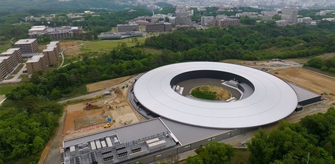
The partnership brings together Rigaku’s expertise in X-ray analytical systems with Tohoku University’s research capabilities. A key part of the collaboration will be the use of NanoTerasu, the university’s next-generation synchrotron radiation facility.
The timing reflects a growing measurement challenge in semiconductor manufacturing. Chip structures are becoming smaller and more layered. Manufacturers are also using a wider range of materials. These changes make it harder to measure structures accurately without damaging them.
X-ray metrology is already used for high-precision, non-destructive analysis. It can provide information about materials and structures without requiring physical destruction of a sample. But conventional approaches face limitations in areas such as microstructure measurement and analysis of structures at different depths.
The new institute will focus on technologies that can address those limitations. One priority is soft X-ray metrology.
Soft X-rays have longer wavelengths and lower energy than conventional X-rays. Their characteristics can make them useful for studying certain materials and structures at small scales. The institute plans to use NanoTerasu’s capabilities to advance this area.
Data analysis will be another major research area. Tohoku University will contribute expertise in information science, while Rigaku will bring its experience in X-ray measurement and instrumentation. The partners aim to combine those capabilities to improve the analysis of increasingly complex measurement data.
The research will initially concentrate on semiconductor applications. The partners want to advance the practical use of soft X-ray metrology and improve data-analysis methods using information science.
The work is expected to expand beyond semiconductors. Electronic materials and functional materials are among the areas that could benefit from more precise measurement of microstructures and material states.
Three-Part Research Strategy
The institute has three main objectives.
The first is to advance X-ray metrology. Researchers will work on new methods for measuring microstructures. NanoTerasu’s soft X-ray capabilities will be combined with Tohoku University’s information-science expertise and Rigaku’s measurement technology.
The second is collaborative research. The institute will investigate X-ray measurement problems across multiple fields. This includes challenges that existing measurement methods cannot adequately address.
The third is talent development. The partners plan to train researchers and engineers in X-ray metrology, from basic principles to applications involving new materials and structures.
The institute is also considering credit-bearing courses. Rigaku’s scholarship system will provide support for graduate students conducting X-ray-related research. The program is designed to connect academic research with practical measurement applications.
That focus on talent is significant because advanced metrology requires expertise across several disciplines. Researchers increasingly need to understand X-ray physics, measurement systems, materials science and data analysis.
The institute is designed to create a stronger link between those areas.
Linking Research With Semiconductor Manufacturing
For the semiconductor industry, measurement is becoming increasingly important as manufacturers push toward smaller dimensions and more complicated device architectures.
The challenge is not limited to seeing smaller features. Manufacturers also need to understand how different materials are arranged within multilayer structures. They need measurements that can provide accurate information without disrupting production or destroying samples.
The institute’s initial research program is therefore closely tied to practical semiconductor requirements. Its work will focus on making soft X-ray measurement more applicable to semiconductor processes while improving the way measurement data is interpreted.
Rigaku, a group company of Rigaku Holdings, has built its business around X-ray analytical technologies. The company sees new measurement requirements as an important driver of further X-ray technology development.
Kazuhiko Omote, General Manager of Rigaku’s X-ray Research Laboratory, will serve as the institute’s Chief Operations Officer and Specially Appointed Professor.
Omote said X-ray technology still has unexplored possibilities despite more than 130 years since its discovery. He said the institute would combine Tohoku University’s academic expertise with Rigaku’s industrial experience while developing the next generation of researchers.
Daichi Chiba, Director of Tohoku University’s International Center for Synchrotron Radiation Innovation Smart, will serve as Operations Support Officer.
Chiba said the institute is intended to connect Rigaku’s technology with the university’s research infrastructure, including NanoTerasu. He also emphasized collaboration across disciplines and between academia and industry.
Why NanoTerasu Matters
NanoTerasu gives the partnership access to advanced synchrotron radiation capabilities. That infrastructure is particularly relevant to the institute’s soft X-ray research.
The facility provides a platform for studying materials and structures using high-performance X-ray techniques. For the new institute, it can serve as a bridge between laboratory research and the development of practical measurement technologies.
The partners will use the initial three-year period to pursue the research themes defined in their joint plan. Results from the semiconductor-focused work will help determine how quickly the program expands into other materials and applications.
The broader ambition is to create a continuing cycle between research, technology development and industrial use.
New measurement challenges from manufacturing can generate research questions. Research can then produce new measurement methods. Training programs can help ensure that the expertise remains available to apply those methods.
That model could become increasingly relevant as semiconductor manufacturing moves into more complex structures and materials.
The institute is scheduled to operate until July 31, 2029, although the partners may extend the collaboration based on its achievements.