

Arizona State University (ASU) will receive $2.062 million in federal funding to develop and test water reuse technologies for semiconductor manufacturing, as Arizona seeks to expand chip production while reducing pressure on its water resources.
The funding was announced by Arizona senators Ruben Gallego and Mark Kelly, along with Representatives Greg Stanton and Yassamin Ansari. The award was made through the National Institute of Standards and Technology (NIST) as congressionally directed spending secured with support from the Arizona delegation.
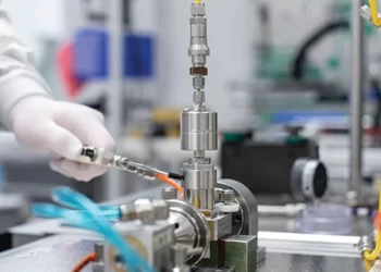
The project will focus on technologies that can treat and reuse water used in semiconductor manufacturing. Researchers will test emerging treatment approaches and demonstrate them at ASU’s Macro Technology Works (MTW) facility in Tempe, where technologies can be evaluated under conditions representative of semiconductor production.
The goal is to generate performance data that manufacturers can use when assessing water-saving technologies for deployment at commercial scale. The project is also intended to improve water conservation at semiconductor fabs while supporting the reliability of domestic chip manufacturing.
“Making Arizona’s semiconductor manufacturing industry even more water efficient will allow us to continue to create good-paying jobs and protect our state’s water supply,” Gallego said.
Kelly said the investment builds on Arizona’s position as a semiconductor manufacturing hub while supporting water conservation, U.S. manufacturing and employment.
Moving water technology toward commercial deployment
The ASU project will advance selected technologies through two development phases. The first will involve developing and integrating emerging water-treatment technologies into a mobile, pilot-scale demonstration testbed.
The second phase will validate those technologies at ASU’s MTW facility under manufacturing-representative conditions. This approach is designed to move technologies beyond laboratory research and establish how they perform in an environment that more closely reflects the demands of semiconductor production.
Quarterly stakeholder reviews will determine which technologies proceed to pilot-scale demonstrations. Researchers will measure water savings, potential cost reductions and operational benefits as part of the evaluation.
The data could help semiconductor manufacturers assess technologies based on measurable performance rather than laboratory results alone. For fabs, water treatment and reuse can be an important consideration in managing manufacturing operations and building resilience in regions where water availability is constrained.
“This investment puts ASU’s researchers to work on exactly the right challenge: making sure the industry driving our economic future can grow without straining the water resources our communities depend on,” Stanton said.
Ansari said the funding would support research, innovation and commercialization aimed at reducing water use and strengthening resilience in Arizona’s semiconductor industry.
Linking semiconductor expansion with water security
Arizona has become an important location for semiconductor manufacturing, with industry investments increasing the state’s role in the U.S. chip supply chain. The expansion has also increased attention on the resources required to support advanced manufacturing.
ASU President Michael Crow said the university intends to use the federal investment to advance technologies that could help semiconductor manufacturers use water more efficiently and strengthen the resilience of chip production in Arizona.
The MTW facility provides a manufacturing-oriented environment for testing the technologies. By validating solutions within a semiconductor manufacturing setting, ASU aims to produce data that can help bridge the gap between fundamental research and commercial adoption.
The project also has a potential commercialization component. ASU expects the research to generate new intellectual property that could be licensed to startups and established water-technology companies.
That could create a pathway for technologies developed or validated through the program to move into commercial products and services, potentially allowing their use across a broader group of semiconductor manufacturing facilities.
For semiconductor fabs, the potential benefits extend beyond reducing water consumption. Technologies that enable greater reuse could help manufacturers improve operational resilience and manage water-related constraints as production capacity expands.
The project reflects a broader effort to address two priorities simultaneously: strengthening domestic semiconductor manufacturing and developing technologies that make that manufacturing more resource-efficient.
With ASU researchers testing treatment technologies under manufacturing-representative conditions, the federal investment is intended to provide the technical and commercial evidence needed to determine which approaches can move toward wider deployment.