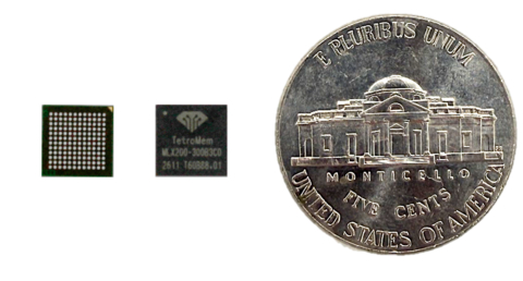
Silicon Valley-based semiconductor firm TetraMem has announced the successful tape-out, manufacturing, and initial silicon validation of its MLX200 platform, a 22nm multi-level RRAM-based analog in-memory computing (IMC) system-on-chip (SoC), marking a significant milestone in the commercialization of next-generation AI computing architectures.
The company said the MLX200 platform integrates multi-level resistive random-access memory (RRAM) arrays with mixed-signal compute engines, enabling vector-matrix operations to be executed directly within memory. The approach is designed to reduce the growing energy and latency costs associated with transferring data between processors and memory in conventional AI systems.
As artificial intelligence workloads continue to scale, the semiconductor industry is increasingly confronting the “memory wall” — a major bottleneck created by the movement of large volumes of data between compute and storage units. Analog in-memory computing is being explored as an alternative architecture capable of improving efficiency by performing computation inside memory arrays rather than relying solely on traditional processor-centric models.
According to TetraMem, the MLX200 platform was fabricated using TSMC’s 22nm process technology. The company said the platform demonstrated several characteristics required for practical deployment, including CMOS compatibility with minimal additional process complexity, low-voltage and low-current operation, strong retention and endurance performance, and high multi-level capability for increased memory and compute density.
Initial silicon validation results reportedly showed consistent functionality across arrays, reinforcing the viability of the architecture for embedded non-volatile memory and compute-in-memory applications.
The milestone builds on TetraMem’s earlier MX100 platform developed on TSMC’s 65nm CMOS process. Previous research by the company demonstrated multi-level RRAM devices capable of supporting thousands of conductance levels, findings that were published in the scientific journal Nature in 2023. Additional work focused on high-precision analog computing using memristor arrays was later published in Science in 2024.
Since 2019, TetraMem has collaborated with TSMC to advance RRAM technology from early-stage research toward manufacturable silicon. The company stated that the progress achieved at the 22nm node reflects continued development in process integration, device uniformity, and system-level co-design.
The MLX200 and MLX201 platforms are aimed at edge AI applications where power efficiency and low latency are critical. Potential deployment areas include voice and audio processing, wearable devices, IoT systems, and always-on sensing technologies.
Evaluated sampling of the platform is expected to begin in the second half of 2026. TetraMem also confirmed that its multi-level RRAM memory intellectual property is available for evaluation and potential licensing.
Dr. Glenn Ge, co-founder and CEO of TetraMem, said the achievement demonstrates the feasibility of bringing multi-level RRAM and analog in-memory computing into advanced-node commercial silicon through close collaboration with TSMC.
The development comes as semiconductor companies globally intensify efforts to create more energy-efficient AI hardware capable of supporting rapidly expanding inference and edge computing workloads.