

Huawei has introduced a new semiconductor development framework called the Tau (τ) Scaling Law, positioning it as a potential successor to Moore’s Law amid growing physical and economic limitations in advanced chip manufacturing.
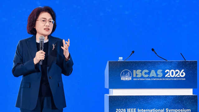
The concept was presented by He Tingbo during a keynote speech titled “New Semiconductor Path in Practice” at the 2026 IEEE International Symposium on Circuits and Systems (ISCAS).
According to Huawei, the τ Scaling Law replaces traditional geometric transistor scaling with “time scaling” as the guiding principle for semiconductor evolution. The company said the approach focuses on reducing signal propagation delay and improving system-level efficiency rather than relying only on shrinking transistor dimensions.
The announcement comes as the semiconductor industry faces increasing challenges in extending Moore’s Law, which has driven chip performance improvements for more than five decades. As transistor miniaturisation approaches physical limits, manufacturers are also dealing with rising fabrication costs and diminishing cost-per-transistor benefits.
Huawei said its τ Scaling framework introduces multi-level optimisation across semiconductor devices, circuits, chips, and computing systems.
At the device level, the company aims to reduce resistance and parasitic capacitance in transistors and interconnects to minimise time delays. At the circuit level, Huawei has developed a new architecture called LogicFolding, designed to shorten critical-path wiring and reduce signal propagation load. The company said this could improve transistor density and circuit performance.
At the chip level, Huawei is using coordinated software, architecture, and silicon design to optimise instruction and data flows. The company said this approach improves parallel processing efficiency and reduces execution time for computing workloads.
At the system level, Huawei introduced a new interconnect technology called UnifiedBus. The company said the technology enables unified memory addressing and lower communication latency across large-scale computing systems and AI infrastructure.
During the keynote, He Tingbo said Huawei has already applied the τ Scaling Law across smartphone and AI computing products. Over the past six years, the company has reportedly designed and mass-produced 381 chips based on the framework for different industries and applications.
Huawei also revealed that its Kirin processors scheduled for launch in Fall 2026 will become the first chips to adopt the LogicFolding architecture. The company claims the technology will deliver significant performance improvements.
Looking ahead, Huawei said its future high-end chips designed using the τ Scaling Law could achieve transistor density comparable to 14 angstrom (1.4nm) manufacturing processes by 2031.
The company also emphasised the need for industry-wide collaboration to sustain semiconductor innovation. He Tingbo said no single company can independently solve the long-term challenges facing semiconductor evolution and called for greater cooperation among scientists, engineers, and industry partners.