

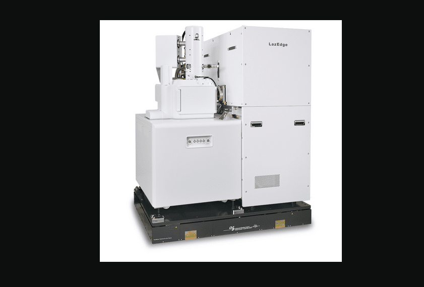
JEOL has announced the commercial launch of LazEdge, a new scanning electron microscope (SEM) system integrated with laser processing technology for high-speed and large-area specimen preparation.
The company said sales of the new system will begin on May 25, 2026.
LazEdge combines JEOL’s SEM platform with proprietary laser technology developed by Hamamatsu Photonics. The system enables laser processing directly inside the specimen chamber of the electron microscope, allowing cross-section preparation and analysis to be performed within a single environment.
According to JEOL, demand has been increasing across research institutes, universities, and industrial sectors for specimen preparation systems capable of processing larger areas at higher speeds while maintaining surface quality.
Traditional cross-section preparation technologies, including focused ion beam (FIB) systems, are widely used for material and semiconductor analysis. However, high-speed preparation of large-area samples remains a challenge in several advanced applications.
JEOL said LazEdge is designed to address those limitations by enabling high-quality cross-section processing with reduced laser-induced periodic surface structures (LIPSS). The company said the system uses a proprietary optical technology capable of spatial phase modulation of the laser beam to improve processing quality inside the SEM chamber.
The platform also features a proprietary shielding technology called “LazEdge Shield.” According to the company, the shield minimizes debris scattering during laser processing and prevents contamination of detectors, specimen chamber walls, and electron columns.
JEOL said the system can simultaneously focus on both the specimen processing point and the laser irradiation position on the shield. This allows cleaning and contamination prevention to occur during operation while maintaining stable laser output.
The company added that performing specimen processing directly inside the SEM chamber enables seamless transitions between processing and analytical workflows. These include SEM observation, elemental analysis, crystal orientation analysis, and electron backscatter diffraction (EBSD) measurements.
LazEdge also supports automated processing and measurement cycles for 3D EBSD data acquisition, according to the company.
JEOL said the system is designed for a range of applications including semiconductor failure analysis, metal specimen analysis, and battery research requiring air-isolated environments.
The company has set an annual sales target of 10 units for the LazEdge system.