

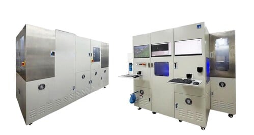
IDI Dynamics has launched a next-generation high-speed laser marking system for semiconductor chip packaging, targeting growing demand for higher manufacturing throughput and improved cleanroom space efficiency in the outsourced semiconductor assembly and test (OSAT) industry.
The company, a subsidiary of ISDN Holdings, said the new IDI Laser Marker delivers up to 2.5 times faster marking speeds compared with widely used industry configurations while reducing physical equipment footprint by 22%.
According to the company, the system has already been deployed at six OSAT facilities across Asia.
IDI said the platform was developed using advanced technologies contributed by a Singapore-based industrial research institution alongside ISDN’s two decades of semiconductor automation engineering experience.
The company stated that benchmarking tests using representative OSAT strip formats and standard marking content showed significant gains in end-to-end cycle time, including strip handling operations.
With faster marking speeds and reduced floor space requirements, the system delivers what the company describes as a 3.2-times improvement in marking productivity per square foot.
Industry analysts note that cleanroom floor space has become increasingly valuable as semiconductor manufacturers expand production capacity to support rising demand driven by artificial intelligence, automotive electronics, industrial automation, and high-performance computing applications.
At the same time, the cost of building advanced semiconductor fabrication and packaging facilities continues to increase globally, pushing manufacturers to maximize productivity within existing facilities.
IDI said the new platform is designed to help semiconductor manufacturers increase output without requiring major cleanroom expansion.
The system also addresses growing traceability requirements in automotive and industrial electronics sectors, where permanent laser marking is increasingly required for quality control, compliance, and supply chain tracking.
According to the company, each system includes a two-year software customization and support program covering factory automation integration, handling adaptations, and evolving compliance coding requirements.
Chris Chan said semiconductor manufacturers are increasingly focusing on balancing throughput and floor space efficiency as demand for advanced chips continues to grow.
He added that the company’s initial deployments are already supporting productivity improvements for OSAT customers in Asia.
Teo Cher Koon said the laser marking platform reflects ISDN’s broader strategy of combining semiconductor engineering expertise, automation systems, and advanced research partnerships to support chip manufacturing productivity.
ISDN said its semiconductor business currently spans a range of products and solutions, including critical components, automation systems, and manufacturing platforms for semiconductor customers across Asia.
The launch comes as OSAT providers continue expanding advanced packaging and testing capacity to support increasing semiconductor demand tied to AI infrastructure, automotive electronics, and next-generation computing technologies.