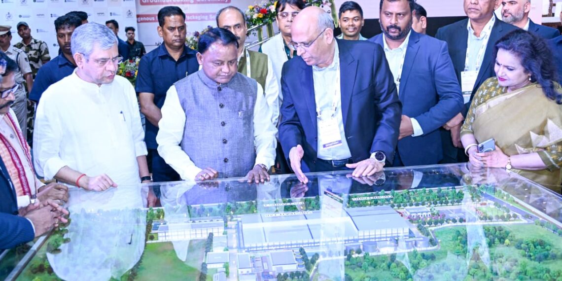
A major step in India’s semiconductor ambitions took shape with the laying of the foundation stone for the country’s first advanced 3D chip packaging facility at Info Valley in Bhubaneswar. The project is expected to strengthen domestic capabilities in high-end electronics manufacturing and support emerging sectors such as artificial intelligence (AI), telecommunications, and defence technologies.
The facility is being set up by 3D Glass Solutions through its Indian subsidiary, Heterogeneous Integration Packaging Solutions Pvt. Ltd. (HIPSPL). Designed as a greenfield, vertically integrated advanced packaging and embedded glass substrate assembly, testing, marking, and packaging (ATMP) unit, it represents a move toward developing critical capabilities in semiconductor back-end manufacturing.
The foundation stone was laid in the presence of Odisha Chief Minister Mohan Charan Majhi and Union Minister for Railways, Electronics & Information Technology, and Information & Broadcasting Ashwini Vaishnaw, alongside senior officials from the central and state governments and industry stakeholders.
Officials indicated that the project is aligned with India’s broader objective of building a resilient and self-reliant semiconductor ecosystem. Advanced chip packaging, a critical segment of the semiconductor value chain, enables the integration of multiple components into compact, high-performance systems, which are increasingly required for next-generation applications.
Speaking at the event, Chief Minister Majhi described the initiative as a significant milestone for Odisha and the country, noting that advanced semiconductor packaging of this nature is being introduced in India for the first time. He stated that the project reflects growing investor confidence in Odisha’s industrial capabilities and policy environment.
The Chief Minister also referred to the global relevance of advanced packaging technologies, citing companies such as Intel, Lockheed Martin, and Applied Materials as key players in the broader ecosystem. Their involvement in similar technologies globally underscores the strategic importance of the segment in the evolving semiconductor landscape.
The total investment in the project is estimated at ₹1,943.53 crore, including ₹799 crore in central fiscal support and approximately ₹399.5 crore from the state government. Once operational, the facility is expected to produce around 70,000 glass panels annually, along with 50 million assembled units and approximately 13,000 advanced 3D heterogeneous integration modules.
These outputs are intended to serve high-growth sectors including data centres, AI and machine learning, 5G and future 6G communications, automotive radar, aerospace, defence electronics, and photonics. Industry observers note that demand across these segments is expected to rise steadily, driven by increasing digitalisation and the expansion of connected technologies.
Union Minister Ashwini Vaishnaw, addressing the gathering, highlighted the growth of India’s electronics manufacturing sector, noting that production has increased six-fold over the past 12 years. He stated that India has emerged as the world’s second-largest mobile phone manufacturer and became the leading exporter of mobile phones in 2025.
The minister added that initiatives under the India Semiconductor Mission are contributing to the development of a more comprehensive semiconductor ecosystem. He confirmed that two semiconductor-related projects have already been approved for Odisha under the programme, with three additional proposals currently under consideration.
He also noted that discussions are ongoing with global companies, including Intel, regarding potential future investments in the state. Such engagements, officials said, could further strengthen Odisha’s position within India’s semiconductor roadmap.
The project is expected to generate employment across a range of skill levels, from engineering graduates to diploma holders and technically trained workers. State authorities indicated that the development of semiconductor infrastructure could also stimulate ancillary industries and contribute to the creation of a broader technology ecosystem.
Odisha, traditionally associated with mineral and metal-based industries, has been working to diversify its economic base. Policymakers have increasingly focused on sectors such as information technology, electronics manufacturing, and semiconductors as part of this transition.
State Minister for Electronics & IT, Dr. Mukesh Mahaling, stated that policy frameworks including the IT, AI, Global Capability Centres (GCC), and Semiconductor Policies 2025 are aimed at attracting investments and fostering innovation. These policies also emphasise workforce development and industry-academia collaboration.
As part of its skill-building initiatives, the state has introduced stipend support for engineering students and is promoting programmes designed to align academic training with industry requirements. Events such as the Blackswan Summit 2026 are also being positioned to attract investment and encourage discussions around emerging technologies, including AI.
Infrastructure development continues to be a parallel focus area. The Union Minister outlined ongoing railway projects in Odisha worth over ₹90,000 crore, along with a record allocation of ₹10,928 crore in the current budget. He noted that 59 stations are being redeveloped under the Amrit Bharat Station Scheme, with efforts underway to expand rail connectivity across all districts.
A proposed four-line coastal rail corridor connecting Balasore to Berhampur is expected to improve logistics efficiency, which is considered critical for manufacturing sectors, including semiconductors that rely on robust supply chains.
According to the project timeline, commercial production at the facility is expected to commence by August 2028, with full-scale operations targeted by August 2030. Industry analysts view the development as a step toward addressing gaps in India’s semiconductor value chain, particularly in advanced packaging, which has traditionally seen limited domestic capacity.
The event was attended by senior officials including S. Krishnan, Secretary, Ministry of Electronics & IT; Anu Garg, Chief Secretary of Odisha; Hemant Sharma, Additional Chief Secretary, Industries Department; Vishal Kumar Dev, Additional Chief Secretary, Electronics & IT Department; and Babu Mandava, Chairman and CEO of 3D Glass Solutions.