

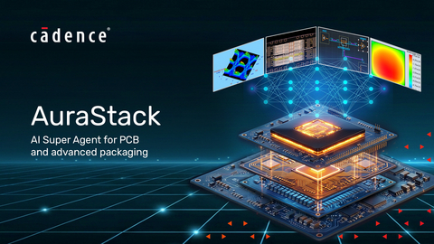
Cadence Design Systems Inc. (Nasdaq: CDNS) has introduced AuraStack AI Super Agent, an agentic artificial intelligence platform designed to automate printed circuit board (PCB) and advanced packaging design workflows, enabling engineers to move from system planning to final product development within a unified AI-driven environment.
The company said AuraStack AI Super Agent is the first agentic AI platform focused on PCB and advanced packaging design. Built on Cadence Allegro AI Studio and accelerated by NVIDIA Blackwell and NVIDIA CUDA-X, the platform coordinates domain-specific AI agents across planning, implementation and multiphysics analysis to streamline electronic system design.
The launch expands Cadence’s AI-based electronic design portfolio, which includes ChipStack, InnoStack and ViraStack AI Super Agents. The company said its agentic AI solutions now span the full electronic system design process, from digital and analog semiconductor design to advanced packaging and PCB development.
“As hyperscale data centers deploy massive AI clusters and other industries advance increasingly intelligent, high-performance systems, engineering teams face growing complexity in PCB and advanced package design,” said Michael Jackson, Corporate Vice President of R&D for System Design and Analysis at Cadence.
He said combining AI-driven orchestration with established electronic design automation and system design analysis tools can help customers move from manual design iterations to more automated engineering workflows.
AuraStack AI Super Agent combines AI capabilities with Cadence’s simulation and optimization technologies to automate design exploration, implementation and verification. The platform supports system planning, constraint management, physical structure definition, intellectual property reuse, routing, design-for-manufacturing analysis and multiphysics optimization.
The platform introduces an integrated multiphysics environment that evaluates electrical, thermal and mechanical performance simultaneously. It can analyze signal integrity, power integrity, thermal performance, mechanical stress, drop impact, vibration and fatigue within a continuous feedback loop.
Cadence said the approach allows engineers to identify potential issues earlier, reduce late-stage redesigns and improve product reliability. The company expects AuraStack to accelerate time to market by up to two times and improve productivity by up to 15 times by automating complex design tasks and expanding design exploration.
The platform integrates Cadence’s existing analysis technologies, including Celsius™ Thermal Solver, Clarity™ 3D Solver for electromagnetic analysis, MSC Nastran™ and Marc™ finite element analysis solvers, and the Sigrity™ X Platform for signal and power integrity analysis.
Cadence is working with several technology companies to apply AuraStack AI Super Agent to real-world engineering challenges. NVIDIA Corporation (Nasdaq: NVDA) is using Cadence solutions to automate and optimize system design workflows for complex AI infrastructure.
Tim Costa, Vice President and General Manager of Computational Engineering at NVIDIA, said modern AI infrastructure requires new approaches to system design. NVIDIA said the combination of Cadence AuraStack AI Super Agent and the NVIDIA Millennium M2000 Supercomputer delivers up to 20 times faster multiphysics performance.
Cadence is also collaborating with Taiwan Semiconductor Manufacturing Co. Ltd. (NYSE: TSM; TWSE: 2330) through its Open Innovation Platform® ecosystem to support AI-driven advanced package implementation for TSMC 3DFabric® technologies.
TSMC said increasing complexity in multi-die systems requires greater automation to achieve faster design convergence. The companies have previously collaborated on substrate auto-routing solutions, enabling customers to improve productivity while maintaining design quality.
Other companies, including Socionext, FORVIA HELLA and Schneider Electric, are applying Cadence AI-based workflows to improve package and PCB design efficiency.
FORVIA HELLA said AI-assisted component placement reduced the time required to place 300 components from up to four days to four minutes, allowing engineers to evaluate more design options during development.