

Great Sky has demonstrated a superconducting AI chip processing high-speed data from a fusion research facility, marking a step toward using specialized neural-network hardware to monitor and control the rapidly changing plasma inside fusion reactors.
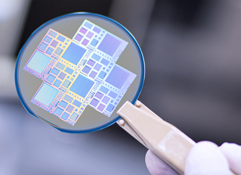
The company worked with Brookhaven National Laboratory, Princeton Plasma Physics Laboratory (PPPL), and the DIII-D National Fusion Facility to develop and test the chip. Unlike conventional central processing units (CPUs) and graphics processing units (GPUs), which use silicon transistors to process digital information, Great Sky’s hardware implements analog neural networks using superconducting circuitry and optical communication.
The team demonstrated the chip on three tasks relevant to tokamak operation. Tokamaks are doughnut-shaped reactors that use magnetic fields to confine hot plasma for fusion research.
Two tests used data collected directly from the DIII-D tokamak to classify anomalies and predict plasma disruptions. The signals were sampled at one million samples per second, and the team reported that the chip processed the data at that rate.
The third test used simulated data generated by TORAX, a tokamak simulator developed by Google DeepMind’s fusion team. The chip processed the signals to predict sawtooth instabilities, recurring changes in plasma conditions that can affect tokamak operation.
Specialized AI hardware targets real-time plasma control
Fusion experiments require fast monitoring because plasma conditions can change rapidly. Control systems must detect developing instabilities and respond quickly to help maintain stable operating conditions.
The latest demonstration provides evidence that Great Sky’s superconducting neural networks can process tokamak data at high sampling rates. The simulated-data test also indicates potential for integrating the hardware into systems that estimate plasma conditions in real time, supporting control and stabilization.
Richard Buttery, director of DIII-D, said the team was encouraged by the chip’s ability to process data from the facility and expressed interest in its potential applications in fusion diagnostics and control.
However, the reported tests do not establish that the chip has been integrated into an operating fusion reactor’s control system. The results demonstrate performance on selected classification and prediction tasks rather than a complete, closed-loop plasma-control system.
Superconducting circuits offer an alternative to silicon
Great Sky has been developing its technology for more than a decade. The work began at the National Institute of Standards and Technology before the team spun out to establish the company.
Its approach combines superconducting electronic circuits with optical communication to implement analog neural networks. The architecture differs from conventional digital AI processors and is intended to improve processing speed and energy efficiency.
These characteristics could be relevant to applications that require rapid analysis of continuous streams of data. Beyond fusion, Great Sky founder and CEO Jeff Shainline identified quantum-system control and error correction, advanced cybersecurity, and video intelligence with continual learning as potential areas for development.
The company has not provided quantitative performance comparisons, power-consumption figures or cost data for the chip in the information released about the demonstration. Its potential efficiency and commercial advantages therefore remain to be assessed against established computing architectures.
Next-generation chip planned for December
The demonstrated device is Great Sky’s largest chip to date, according to Shainline. The team plans to demonstrate a next-generation chip in December, featuring a neural network 10 times larger than the current version.
The planned development will test whether the architecture can scale while retaining the processing capabilities needed for demanding scientific applications.
The collaboration brings together specialized computing hardware and fusion research infrastructure to address a practical challenge: extracting useful information from plasma measurements quickly enough to support control decisions. Further testing will be needed to establish how the technology performs in operational environments and whether it can deliver reliable, energy-efficient control at the scale required by future fusion systems.