

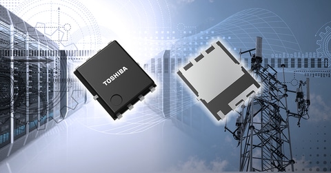
Toshiba Electronic Devices & Storage Corporation has launched a new 80V N-channel power MOSFET designed to improve power efficiency in AI data centers and communications infrastructure, as operators seek to reduce energy consumption and manage increasing compute workloads.
The new device, TPM1R408RH, is manufactured using Toshiba’s latest U-MOS11-H process technology and is targeted at switched-mode power supplies used in industrial equipment, AI data centers and communications base stations. Shipments began on Tuesday, the company said.
The launch comes as rapid growth in artificial intelligence applications drives higher power requirements across data centers, increasing demand for power semiconductors capable of reducing energy losses, minimizing heat generation and supporting higher power density. These requirements have also intensified the need for improved thermal management and lower electromagnetic interference (EMI) in power supply systems.
According to Toshiba, the TPM1R408RH delivers a maximum drain-source on-resistance of 1.4 milliohms, approximately 26% lower than its previous-generation 80V MOSFET, the TPM1R908QM, which was built using the company’s earlier U-MOS X-H process.
The company also said the new device improves the balance between on-resistance and total gate charge, reducing its figure of merit—measured as RDS(ON) multiplied by gate charge—by around 45% compared with its predecessor. Lower values typically translate into reduced conduction and switching losses, contributing to improved power conversion efficiency in high-performance systems.
Beyond efficiency gains, Toshiba said the MOSFET suppresses voltage spikes generated during switching operations, helping reduce electromagnetic interference in switched-mode power supplies. Lower EMI can simplify circuit design by reducing the need for additional filtering and snubber circuitry, potentially shortening development cycles for power supply manufacturers.
The device is packaged in Toshiba’s SOP Advance(E) package, which the company said reduces package resistance by approximately 65% and thermal resistance by about 15% compared with its existing SOP Advance(N) package. The improved thermal performance is intended to support higher output power while enabling more compact power supply designs.
To support product development, Toshiba has also expanded its design ecosystem with SPICE simulation models and an online circuit simulator. The web-based tool allows engineers to evaluate circuit performance directly through a browser without installing dedicated simulation software or downloading device models.