The UCLA Samueli School of Engineering has launched a $125 million Semiconductor Hub, bringing together some of the biggest names in the semiconductor and technology industries to accelerate research, innovation, and workforce development in artificial intelligence-driven chip technologies.
The founding members include Broadcom Inc. (NASDAQ: AVGO), Applied Materials Inc. (NASDAQ: AMAT), GlobalFoundries Inc. (NASDAQ: GFS), Meta Platforms Inc. (NASDAQ: META), and Synopsys Inc. (NASDAQ: SNPS). The initiative is backed by an initial five-year commitment comprising philanthropic contributions and in-kind support.
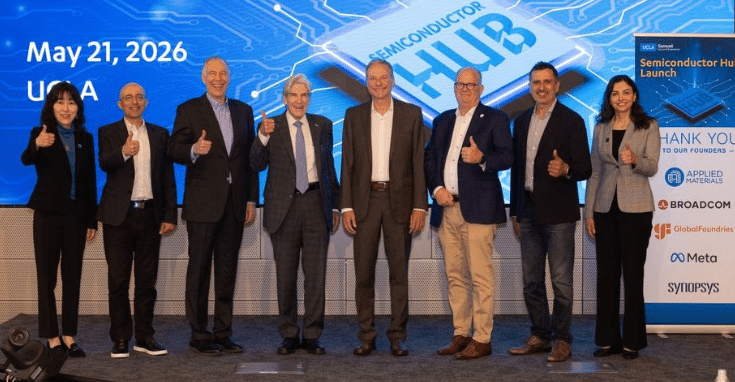
The hub was formally unveiled at an event hosted by UCLA Samueli. Attendees included industry executives, faculty members, doctoral students, media representatives, and policymakers. UCLA Chancellor Julio Frenk, former California Governor Gray Davis, and Henry Samueli, chairman of Broadcom and the engineering school’s namesake, were among those present.
The new center aims to create long-term collaboration across the semiconductor value chain, covering chip design, manufacturing, software, equipment, advanced materials, and packaging technologies.
The launch comes as demand for AI computing continues to drive investment in next-generation semiconductor technologies. Industry leaders increasingly view collaboration between academia and industry as critical to overcoming technical barriers and addressing future talent needs.
“UCLA is uniquely positioned to bring together expertise across disciplines to push the frontiers of semiconductor innovation and translate that knowledge into scalable solutions,” said Julio Frenk.
“The Semiconductor Hub at the UCLA Samueli School of Engineering reflects our commitment to forging partnerships with industry in a field critical to economic vitality and national security.”
According to UCLA, the hub will focus on advancing semiconductor and AI technologies through a co-design approach that integrates materials, devices, software, and system architectures.
Research efforts will target AI-native hardware and software systems, advanced packaging, thermal management, ultra-broadband connectivity, and energy-efficient computing. The goal is to move beyond traditional silicon scaling limits and enable new computing architectures capable of supporting future AI workloads.
Ah-Hyung Park said the idea for the hub emerged from discussions with Henry Samueli.
“The vision for the Semiconductor Hub took shape after a conversation with Henry Samueli, one of the most influential innovators of our time,” Park said.
“Henry cofounded Broadcom while teaching at UCLA, underscoring the school’s strong position to help drive semiconductor innovation for a new era of AI.”
The initiative also seeks to strengthen U.S. competitiveness in semiconductor technologies. Organizers said the hub will bring together expertise from across the industry to help accelerate innovation and shorten the path from research to commercialization.
Charlie Kawwas, president of Broadcom’s Semiconductor Solutions Group, described the hub as a comprehensive collaboration spanning multiple segments of the semiconductor ecosystem.
“We’re proud to join our founding partners in launching the Semiconductor Hub,” Kawwas said.
“Through deep industry-academia collaboration, we are empowering the next generation of engineers and researchers to drive global innovation and tackle the world’s most pressing challenges.”
The hub’s research agenda extends beyond conventional semiconductor technologies. Planned areas of exploration include real-time artificial general intelligence inference at the edge, self-optimizing data centers, and next-generation communication systems operating across radio frequency, terahertz, and optical domains.
These technologies could support future applications in autonomous vehicles, robotics, environmental monitoring, healthcare, and space-based systems.
Meta highlighted the growing importance of semiconductor innovation in enabling the next wave of AI development.
“At Meta, we’re investing in the foundational technologies that will power the next era of AI,” said Yee Jiun Song.
“UCLA’s Semiconductor Hub is tackling some of the most important challenges in computing, from energy-efficient chip design to advanced packaging.”
GlobalFoundries President and CEO Tim Breen said advanced semiconductors are becoming increasingly important across both data-center and edge AI environments.
“The technologies shaping the next decade all depend on advanced semiconductors,” Breen said.
“As a founding member of UCLA’s Semiconductor Hub, GF is proud to work alongside leading researchers and partners to tackle the industry’s toughest challenges.”
Synopsys President and CEO Sassine Ghazi emphasized the growing need to integrate hardware and software development.
“Engineering technology’s future demands co-design of software and hardware, electronics and physics, from silicon to system,” Ghazi said.
Applied Materials President and CEO Gary Dickerson said industry-academic collaboration is becoming increasingly important as semiconductor complexity grows.
“Strengthening the ties between industry and academia is more important than ever,” Dickerson said.
Beyond research, workforce development is a central pillar of the initiative. The hub will support doctoral students conducting semiconductor research at UCLA while offering yearlong internships with founding member companies.
The center will be led by Mona Jarrahi and supported by a multidisciplinary team of UCLA researchers.